Energy Sector Millimeter Band RF Waveguide Measurements Using High-Resolution 3D Scanning
Executive Summary
High-frequency millimeter band RF waveguides require strict dimensional accuracy and surface integrity to ensure optimal signal transmission. EDM Intelligent Solutions provides high-resolution, non-contact 3D metrology services that allow for comprehensive form and surface inspection at the micron level. This report highlights the application of 3D scanning and CAD comparison to evaluate a copper alloy microwave RF waveguide component using our MVi5 3D Metrology Center.Overview of 3D Metrology Capabilities
Using optical scanning technologies, EDM Intelligent Solutions provides in-depth geometric inspection, surface deviation analysis, and full CAD comparison for high-precision components. Form measurements are derived from 2D cross-sectional profiles taken from 3D scan data, while difference measurement overlays scan data onto the nominal CAD model to create visual deviation maps. Key capabilities include:- µm-level 3D scanning and form measurement
- Difference measurement for full CAD comparison and tolerance mapping
- Optical surface mapping and defect visualization
- Tolerance band overlays for conformance reporting
Application Case Study: Millimeter Band RF Waveguide Inspection
Component Overview
- Type: Millimeter Band Microwave RF Waveguide
- Material: Copper Alloy
- Metrology System: MVi5 3D Metrology Center
- Metrology Services: Form Measurement, Difference Measurement, Optical Surface Mapping, Tolerance Band Visualization
Inspection Process
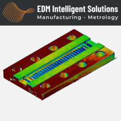
The waveguide component was scanned using the MVi5 3D Metrology Center to create a high-resolution 3D mesh. Profile slices were taken from the mesh to measure key geometric features such as radii, angles, step heights, and slot widths. Following profile analysis, the scanned data was compared to the nominal 3D CAD model using difference measurement techniques. This overlay generated a full-surface deviation map with color-coded tolerance zones, allowing engineers to easily identify areas of non-conformance and critical form deviations. Visual tools were used to magnify specific sections of the component for closer inspection and documentation of any localized deviations or anomalies.Results & Value Delivered
- Complete, non-contact inspection of complex RF waveguide geometry
- CAD-to-part deviation analysis with visual tolerance mapping
- Detection of minor form discrepancies in critical transmission zones
- Traceable documentation supporting high-frequency design validation
Conclusion
RF waveguides operating at millimeter band frequencies demand ultra-tight tolerances and defect-free surfaces to maintain signal fidelity. EDM Intelligent Solutions delivers accurate and repeatable 3D metrology solutions to support dimensional validation and CAD comparison for these critical components. Our MVi5 system enables rapid feedback and quality assurance for energy and communications technology manufacturers.About EDM Intelligent Solutions
EDM Intelligent Solutions is a trusted provider of advanced manufacturing and metrology services for industries including energy, aerospace, medical, and electronics. We specialize in high-resolution, non-contact 3D inspection systems that provide digital insights for process control, defect detection, and dimensional conformance.Downloadable PDF of Applications Report