Electronics Form Scan and Dimensional Analysis of Printed Circuit Boards (PCBs)
Executive Summary
As the demand for miniaturized and high-performance electronics continues to grow, ensuring the dimensional accuracy of printed circuit boards (PCBs) becomes increasingly critical. EDM Intelligent Solutions offers high-resolution, non-contact 3D metrology services that allow for precision inspection of PCB surfaces and geometries. This report outlines our four-step form scan methodology using the MVi5 3D Metrology Center for PCB inspection.
Overview of 3D Metrology Capabilities
Our metrology systems provide µm-level resolution and support in-depth, non-destructive dimensional measurement of PCBs and other electronic components. Using 3D profile slicing, we extract detailed measurements of features such as slot widths, hole positions, step heights, radii, and angles—ensuring complete geometric verification.
Key capabilities include:
- Non-contact 3D form scanning with micron precision
- Cross-sectional analysis of PCB height, slot geometry, and surface flatness
- Measurement of warpage, deformation, and bow
- Support for component alignment and assembly verification
Application Case Study: PCB Form Scan
Component Overview
- Type: Printed Circuit Board
- Material: FR4 (Printed Circuit Board)
- Metrology System: MVi5 3D Metrology Center
- Metrology Service: Form Measurement
Form Scan Inspection Process
Step 1: Capture Full 3D Data
The MVi5 3D Metrology Center performs a non-contact scan of the PCB to generate a full 3D point cloud. This scan captures fine geometric features and surface topography at the micron scale.
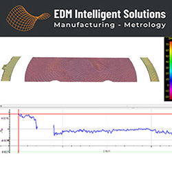
Step 2: Generate Cross-Sectional Profiles
From the 3D data, multiple cross-sectional profiles are created through key PCB areas. These profiles reveal vertical step changes, slot depths, hole positions, and alignment features.
Step 3: Form Measurement and Analysis
Critical dimensional values such as planarity, warpage, and edge alignment are measured using the extracted profiles. Tolerances are verified against design specifications.
Step 4: Reporting and Documentation
Measurement results are compiled into a digital inspection report, with dimensional visuals and tabulated data. This ensures traceability for quality assurance and process validation.
Results & Value Delivered
- Accurate form measurement of complex PCB features
- Detection of bow, warp, or deformation during manufacturing
- Non-destructive analysis ideal for sensitive electronic materials
- Supports traceability and documentation for quality audits
Conclusion
EDM Intelligent Solutions’ 3D metrology capabilities offer electronics manufacturers the ability to detect dimensional issues early, ensure conformance to design, and improve product reliability. Our advanced form scan methods provide actionable data with the precision and reliability required for modern PCB inspection.
About EDM Intelligent Solutions
EDM Intelligent Solutions provides advanced metrology and precision manufacturing services for the electronics, aerospace, medical, and scientific sectors. Our non-contact inspection technology and automated measurement systems support high-quality production and quality assurance programs.
Downloadable PDF of Applications Report
Let’s Discuss Your Application
Have a challenging measurement problem? Our engineers are ready to help.